Engineers are turning to packaging substrates to optimize electronic devices in preparation for an era that relies heavily on big data and computationally enormous artificial intelligence algorithms.
One specific branch of packaging substrate research aims to find a scalable solution that will shift the semiconductor industry from carbon-based substrates to glass. Glass substrates aren’t new, but their use has picked up steam as major tech companies plan next-generation releases for the latter part of this decade, with Intel leading the charge. Here’s why.
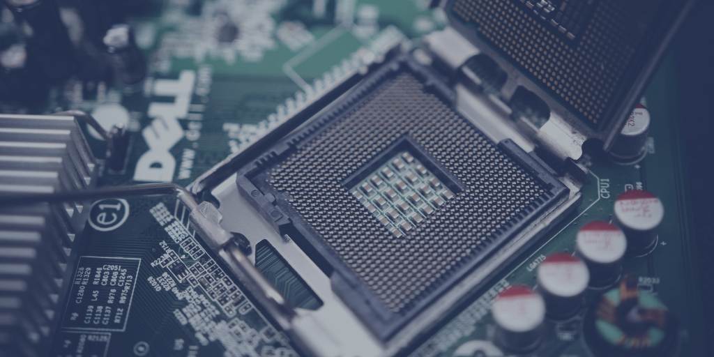
It’s no contest between carbon and glass substrates in terms of performance.
Georgia Tech’s 3D Systems Packaging Research Center (PRC) is the largest academic center in the world that focuses on advanced packaging. The PRC is a National Science Foundation Engineering Research Center that collaborates with 14 universities and 48 government and industry organizations, including Intel. In fact, Intel Fellow Dr. Ravi Mahajan was one of the PRC’s initial Industry Advisory Board members announced in 2022. A full list of big-name collaborators hints at the scale that this technology is likely to be deployed once all the kinks are worked out.
PRC Director, Madhavan Swaminathan, describes seven key benefits of glass over traditional, organic (carbon-based) substrates, including:
- smoothness, which enables dense connectivity between chips;
- tailorable thermal expansion, which improves reliability;
- stiffness, which eases manufacturability;
- zero moisture absorption, which improves stability;
- low thermal conductivity, which isolates hotspots;
- dielectric insulation, which improves performance;
- and large-area panel processing, which reduces cost.
In academia, these factors could enable novel research in disciplines spanning computer science, aerospace, engineering, biomedical — pretty much any field that requires (or would benefit from) computational analysis. In industry, glass substrates could be particularly impactful for high-performance computing, high-temperature environments such as automotive or aerospace, 6G wireless, and miniaturized consumer electronics.
“The PRC has been pioneering glass substrate technology for many years,” says Swaminathan. “With applications emerging in artificial intelligence, high-performance computing, and high-end communications, we expect glass substrates as being the next technology of the future.”
So if glass substrates undeniably outperform organic substrates, why has it taken so long for companies to shift gears to glass?
This is why we can’t have nice things — yet.
The downside is that glass electronics have to be handled like they’re…well, made of glass. When Apple first released its iPhone fitted with external glass components, consumers were concerned — if not downright mad. They saw glass products as a tactic that would cause them to need to replace already expensive consumer electronics more frequently.
That consumer backlash hasn’t stopped Apple. The tech titan has been racking up patents for glass electronics for years, including an all-glass iPhone. As one commenter responded to the news, it’s easy to picture the all-glass iPhone as having “all the ergonomics of a bar of soap,” which is exactly what manufacturers fear in the manufacturing and assembling stages of glass substrates. Or, as Intel put it, their priority is “basically, saving glass from itself.”
Srini Pietambaram, Principal Engineer and Module Engineering Pathfinding Lead on the Substrate Packaging Technology Development team at Intel, says they’re working on designing a manufacturing ecosystem that will be able to handle the glass substrates produced at mass volume.
There’s no doubt that as research progresses glass substrate functionality will continue to be refined and scaled to meet Intel’s goal to deliver 1 trillion transistors on a package utilizing glass substrates by 2030. For now, we’ll have to be content with this video footage from inside Intel’s Assembly and Test Technology Development factory.
Read more: