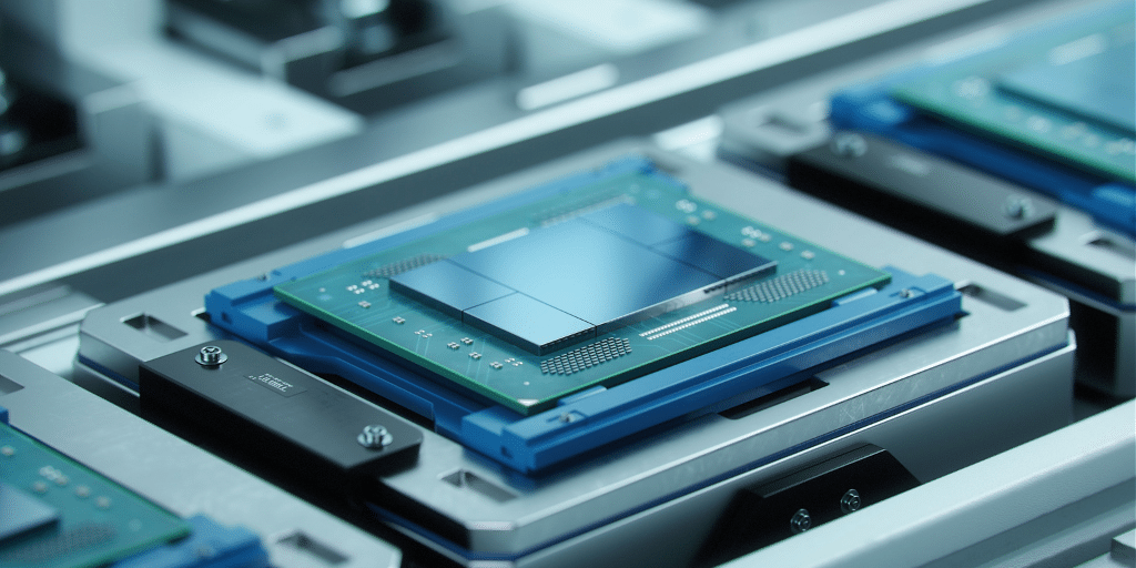
The future of semiconductors may rely less on the technology of the chips themselves and more on how they are packaged.
As performance demands continue to grow, chipmakers are exploring new ways to squeeze more functionality into the same limited space. Chip packaging has gone from almost an afterthought to being a key driver of new semiconductor technology.
What is advanced chip packaging?
Packaging used to be one of the last steps in semiconductor manufacturing. Chips were sealed inside protective packages, which served the dual purpose of preventing corrosion and providing an interface to connect to other chips. But as chip technology continues to march forward at breakneck speed, chip packaging has become more advanced—and taken on a much more significant role.
Chips have been rapidly shrinking over the last few decades, but they’re starting to reach the limit of what is feasible to manufacture. Even the most highly integrated monolithic chips, which are packed with components and functionality, can’t keep up with the demands of today’s cutting-edge technologies. The alternative? Multi-die design, which partitions chips into smaller pieces called chiplets, then integrates them in the packaging step.
This modular approach comes with several benefits. Integrating chiplets vertically into 2.5D or 3D ICs allows designers to continue shrinking the chip’s footprint for cutting-edge applications. Designers also have more flexibility, mixing and matching chiplets with different functions and even chiplets from different manufacturers. The design process is simplified because it’s no longer about designing a whole new chip; it’s about taking existing chiplets and organizing them in new ways. Thus, multi-die design makes the design stage simpler, faster, and more affordable. The modularity also improves yields. In the past, a single speck of dust could contaminate an entire monolithic chip. Now, if one chiplet is contaminated, it can be replaced more easily and cheaply than the entire system.
The packaging arms race
As the ability to shrink chips approaches current physical limits, the race for technological innovation has turned to packaging. Designers and manufacturers are embracing multi-die design and pouring resources into advanced chip packaging. The result? A packaging “arms race” with Intel, Samsung, and TSMC at the forefront. These companies saw where the industry was headed and started investing in packaging nearly a decade ago. In that time, TSMC has patented nearly 3,000 advanced packaging technologies; Samsung follows with around 2,400 and Intel with 1,400.
Their efforts have paid off: they’re now the only companies in the world with the technology to package the most cutting-edge chips. Samsung took their commitment to advanced chip packaging a step further in 2022, when they created a dedicated team for it. In 2023, TSMC opened its first all-in-one advanced packaging and testing plant to mass produce its SoIC and 3DFabric packaging technologies for applications like AI and data centers.
How are chipmakers thinking about chip packaging now?
As the advanced chip packaging arms race heats up, some companies are carving out specific niches to try to distinguish themselves. For instance, Intel’s packaging is targeted for high-performance computing applications, in line with Intel’s position as a world leader in the cloud and computer industries. Samsung, on the other hand, has focused its packaging efforts on high-volume assembly applications. TSMC has taken a broader approach, working with a variety of customers in an attempt to develop the world’s most comprehensive packaging solutions.
Besides being the next horizon in innovation, advanced chip packaging offers another benefit to companies that embrace it: built-in brand loyalty. Advanced packaging allows customers to become foundry-independent, because the design is no longer in the chips (or, nowadays, chiplets) but rather in how they’re packaged together. Chiplet packaging, on the other hand, is deeply complex and foundry-specific. Once a customer qualifies a modular packaging system, they’ll want to design future products within the same system—and thus the same manufacturer. Companies like Intel, Samsung, and TSMC hope that investing heavily in packaging now will help them win over customers for years to come.
As the industry continues to embrace multi-die design, advanced chip packaging will only become more widespread and more vital to chipmakers vying for business. Though the packaging race has so far been dominated by three industry giants, it’s likely we’ll see more companies entering the race in the coming years—and even more impressive innovations as a result.
Read more:


